According to the experience of
PCB manufacturing, this paper summarizes the contents that need to be checked after the completion of PCB design:
1. Check the high-frequency, high-speed, clock and other fragile signal wires to see if the loop area is the smallest, if they are far away from the interference source, if there are redundant vias and wires, and if there are broken strata division areas.
2. Check whether there is a signal line under the crystal, transformer, optical coupler and power supply module, and try to avoid threading under it, especially laying grounding copper sheet under the crystal.
3. Check whether the positioning holes and positioning parts are consistent with the structural drawing, and whether the ICT positioning holes and SMT positioning cursor are added and meet the process requirements.
4. Check whether the serial number of the device is placed correctly according to the principle of from left to right, and there is no silk screen covering pad; check whether the version number of the silk screen is in line with the version upgrade specification and mark it.
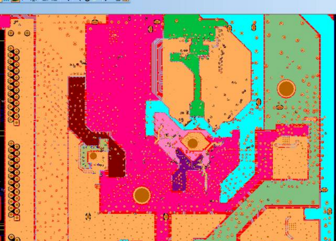
5. Report whether the wiring is 100%, whether there are wire ends, and whether there are isolated copper sheets.
6. Check that the power supply and ground are separated correctly; single point and common ground have been treated.
7. Check that the light drawing options of each layer are correct, and the labels and light drawing names are correct; if the panel needs to be assembled, only the drawings of the drilling layer need to be marked.
8. Output the photo file and check with CAM350 to confirm that the photo file is generated correctly.
9. Fill in the
PCB layout (filing) self inspection form as required, and submit it to the process designer together with the design documents for process review.
10. Actively improve the problems found in the process review to ensure the manufacturability, producibility and testability of veneer.