Allegro PCB design – Gerber output settingsAdd photo drawing layer manually
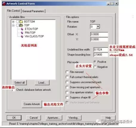
Output the photo drawing command in the menu manufacture = > artwork or click the toolbar icon. The open window is as follows:
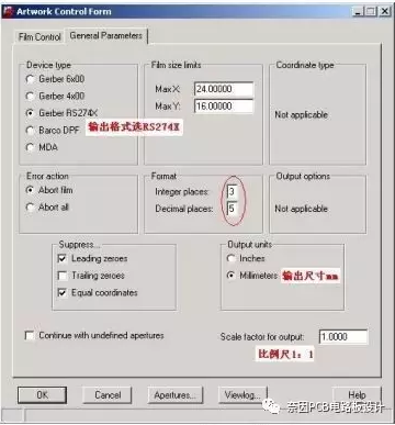
The above figure is the layer control window of photo output, and another window is the control window of output parameters. We can open the window by clicking the second list item general parameters in the above figure. The open window is as follows. Note that rs274x is selected as the output format.
The default output photo layer list of Allegro software includes two items: top and bottom. We need to add them according to the corresponding board layers. Taking a four layer PCB as an example, when there are no components in the bottom layer, eight photo files (actually 7 films, drilling is not considered as film in PCB manufacturers) are needed. The eight gerber files are as follows:
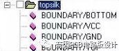
Topsilk
Topmask
Top
Gnd
Vcc
Bottom
Botmask
Drill
If the components are placed on the bottom layer, there is also a layer of botsilk. Through the description above, I believe you have a certain understanding of how to calculate the number of gerber files output. The following describes the relevant layers that need to be opened when outputting each layer of gerber files on this PCB:
1. Topsilk
lREF DES/SILKSCREEN_ TOP
lPACKAGE GEOMETRY/SILKSCREEN_ TOP
lBOARD GEOMETRY/OUTLINE
2. Topmask
lVIA CLASS/SOLDERMASK_ TOP
lPIN/SOLDERMASK_ TOP
lPACKAGE GEOMETRY/SOLDERMASK_ TOP
3. Top
lETCH/TOP
lPIN/TOP
lVIA CLASS/TOP
4. GND layer (GND)
lETCH/GND
lPIN/GND
lVIA CLASS/GND
5. VCC layer (VCC)
lETCH/VCC
lPIN/VCC
lVIA CLASS/VCC
6. Bottom wiring
lETCH/BOTTOM
lPIN/BOTTOM
lVIA CLASS/BOTTOM
7. Bottom solder mask
lVIA CLASS/SOLDERMASK_ BOTTOM
lPIN/SOLDERMASK_ BOTTOM
lPACKAGE GEOMETRY/SOLDERMASK_ BOTTOM
8. Drill
lMANUFACTURING/NCDRILL_ LEGEND
lMANUFACTURING/NCDRILL_ FIGURE
lBOARD GEOMETRY/OUTLINE
lBOARD GEOMETRY/DIMENSION
Next, we will set the Gerber of each layer according to the above list. The specific operation steps are as follows:
1. Run the command manufacture = > Artwork or click the toolbar icon.
2. Right click the “top” character in the photo output list and select the add command in the pop-up menu.
3. Enter “topsilk” in the pop-up window and press OK to close the window (add top screen printing)
4. Click “+” at the front of topsilk layer to open the list item, as shown in the following figure:
5. Use the “cut” and “add” commands of the right mouse button menu to delete the useless layers and add the layers related to silk screen printing, namely ref DES / silkscreen_ TOP??PACKAGE GEOMETRY/SILKSCREEN_ Top and board geometry / outlook
6. Use the same method to set other layers of light drawing, and refer to the list above for relevant layers
7. Set the undefined line width of all layers to 0.1524
8. Set the shape bounding box of all layers to 2.54
9. Set the GND and VCC layers to negative, and select negative in plot mode
The bottom of the selected vector has been output
11. Set the parameters of general parameters as shown in Figure 3.20
12. Click OK to close the artwork control form window
At this time, if we look at the views option in the visibility parameter on the right, we can see the Gerber output layer list as shown in the following figure:
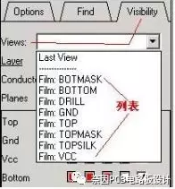
In fact, the output of Gerber should be set before routing. In this way, in the subsequent routing process or other processes, the relevant layers can be quickly switched through the views list under the visibility parameter on the right side of allegro. For example, if I want to route in the bottom layer, and I want to turn off the display of other layers, we can select from the views list Bottom, all other layers are closed and only the bottom layer is kept.
Output Gerber file
Next, you can output the Gerber file. Check the parameter settings. If the parameters are OK, click the “select all” button to select all layers, and then click the “create art” button to start photo output. The extension of the generated Gerber file is “art”, and the files are stored in the physical directory, We put these art files together with drill holes ncdrill1.tap and nctape.log File compressed into rar (compression software) file, with this compressed rar file can be
PCB production.
After the output of the Gerber file, we suggest that you use CAM350 and other software to edit and view the Gerber file to check whether there are errors in the output Gerber file.


