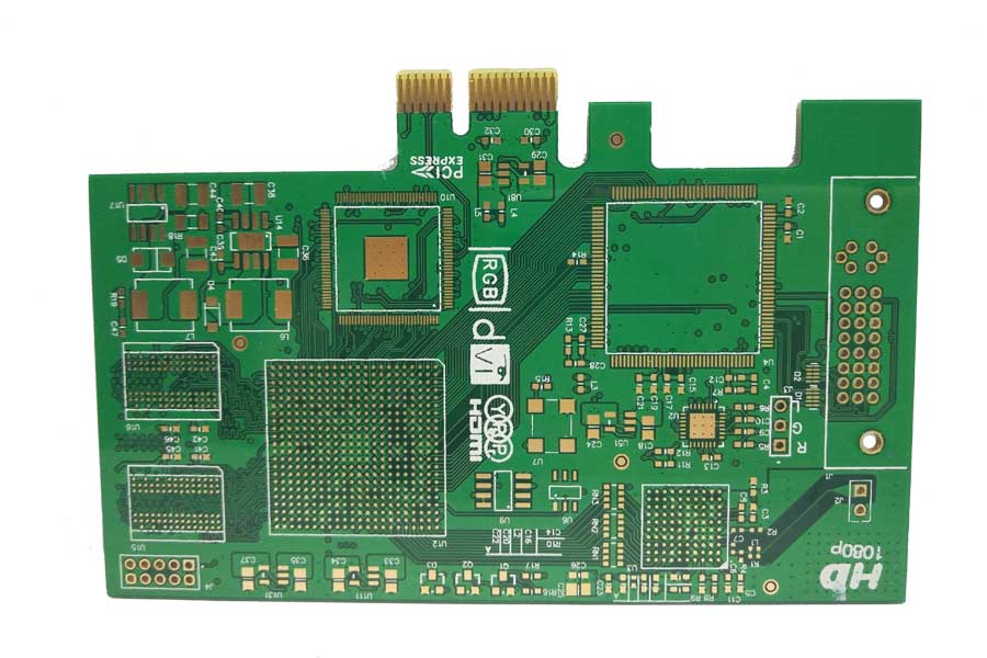
Goldfinger PCB: insert one end of PCB board into connector slot, use connector socket as the outlet of external connection of PCB board, make the pad or copper skin contact with the socket foot of corresponding position to achieve the purpose of conduction, and plating nickel and gold on the pad or copper skin of PCB board. It is called the golden finger because it is shaped like a finger. Gold is chosen because of its excellent electrical conductivity, oxidation resistance and wear resistance. But because of the high cost of gold, it can only be applied to local gold plating such as Goldfinger PCB.

Classification, recognition and characteristics of Goldfinger PCB
Goldfinger PCB classification: regular golden finger (flat finger), long and short golden finger (uneven golden finger), segmented golden finger (intermittent golden finger).
1. Conventional golden finger: A rectangular pad with the same length and width is arranged neatly at the edge of the plate. The following picture is: network card, graphics card and other types of physical objects, more golden fingers. Some small plates have fewer golden fingers.
2. Golden finger: a rectangular pad with different lengths at the edge of the plate
3. Segmented golden finger: a rectangular pad with different lengths at the edge of the plate, and the front segment is disconnected.
There is no character box and label. It is normal to open a window for the solder barrier layer. Most shapes have grooves. The golden finger part protrudes or approaches the edge of the board. Some boards have golden fingers at both ends. Normal golden fingers are on both sides. Some PCB boards have only one golden finger. Some golden fingers are single and wide.
At present, the commonly used gold finger plating process mainly has the following two kinds:
One is to lead from the end of the golden finger. As a gold-plated wire, the lead is removed by milling or etching after the gold-plating is completed. However, the products produced by this process will have residual lead around the golden finger, resulting in copper dew, which can not meet the requirement of not allowing copper dew.
The other is not to lead from the golden finger, but from the inner or outer circuit of the circuit board connected with the golden finger to achieve gold finger plating, thus avoiding copper exposure around the golden finger. However, when the line density in the circuit board is very high and the line is very compact, it may not be possible to make the lead in the circuit layer using this technology; moreover, this technology can not do anything for the isolated golden finger (i.e., the golden finger is not connected to the line).