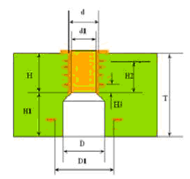
1. What back drill?
In fact, back drilling is a special kind of depth control drilling. In the production of multi-layer pcb boards, such as the production of 12-layer pcb, we need to connect the first layer to the ninth layer. Usually, we drill via holes (once drilling), and then aging copper. In this way, the first layer is directly connected to the 12th layer. In fact, we only need to connect the first layer to the ninth layer. Because there is no line connected from the 10th to the 12th layer, it is like a column. This pillar affects the signal path, which can cause signal integrity problems in communication signals. So drill this extra column (called stub in the industry) from the opposite side (secondary drilling). Therefore, it is called back drilling, but it is generally not as clean as drilling, because a little copper will be electrolyzed in the subsequent process, and the drill point itself is also sharp. Therefore, the PCB manufacturer will leave a small point. The length of the stub left is called b value, which is generally good in the range of 50-150um.
2. What are the advantages of back drilling?
a. Reduce noise interference;
b. Improve signal integrity;
c. The thickness of local plate becomes smaller;
d. Reduce the use of blind holes, reduce the difficulty of PCB production.
3. What is the function of back drilling?
The function of back drilling is to drill out the through-hole section which has no connection or transmission function, so as to avoid the reflection, scattering and delay of high-speed signal transmission, and bring "distortion" to the signal. The research shows that the main factors affecting the signal integrity of signal system are design, material, transmission line, connector, chip package and other factors ??
4. Working principle of back drilling
The micro current generated when the drill needle contacts the copper foil on the substrate surface to induce the height position of the board surface when the drill needle is running in the hole, and then the drill in is carried out according to the set drilling depth, and the drilling is stopped when the drilling depth is reached.
5. What is the main application field of back drilling PCB?
Back drilling PCB is mainly used in communication equipment, large server, medical electronics, military, aerospace and other fields. As military and aerospace are sensitive industries, domestic backboards are usually provided by research institutes and R & D centers of military and aerospace systems or PCB manufacturers with strong military and Aerospace background; in China, the demand for backplanes mainly comes from the communication industry, and now the communication equipment manufacturing field is gradually growing.