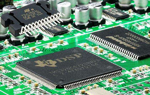
Digital signal processing chip (DSP) has high-performance CPU (clock performance over 100MHz) and high-speed advanced peripheral equipment. With CMOS processing technology, DSP chip power consumption is getting lower and lower. These great progress increases the complexity of DSP circuit board design, and compared with simple digital circuit design, it faces more similar problems.
The following is the DSP hardware PCB design considerations, colleagues can refer to.
Selection principle of clock circuit:
1. When multiple clock signals with different frequencies are required in the system, the programmable clock chip is preferred;
2. When the clock signal is single, the crystal clock circuit is selected;
3. When there are multiple clock signals of the same frequency, the crystal oscillator is selected;
4. Try to use the PLL in DSP chip to reduce the off chip clock frequency and improve the stability of the system;
5. There is no oscillation circuit in the DSP chip such as C6000, c5510, c5409a, c5416, c5420, c5421 and c5441, so the crystal clock circuit cannot be used;
6. The level of vc5401, VC5402, vc5409, f281x and other DSP clock signals is 1.8V, so crystal clock circuit is recommended.
Disposal of unused input / output pins
1. Unused input pins should not be suspended, but should be pulled up and pulled down to a fixed level
1) The key control input pins, such as ready and hold, should be fixed in the appropriate state, the ready pin should be fixed in the effective state, and the hold pin should be fixed in the invalid state
2) No connection (NC) and reserved (RSV) pins, NC pins: unless otherwise specified, these pins are suspended, RSV pins: whether to connect or not should be determined according to the data manual
3) For non critical input pins, pull them up or down to a fixed level to reduce power consumption
2. Unused output pins can be suspended
3. Unused I / O pin: if the save status is input pin, it will be treated as non critical input pin, and pull-up or pull-down is fixed level; if the save status is output pin, it can be suspended
Why DSP with large on-chip RAM has high efficiency?
At present, the ram of DSP is becoming larger and larger. In order to design an efficient DSP system, DSP with larger ram should be selected. Compared with off chip ram, on-chip RAM has the following advantages:
1) The speed of on-chip RAM is fast, which can ensure DSP running without waiting.
2) For C2000 / C3x / C5000 series, some on-chip memory can be accessed twice in one instruction cycle, which makes instructions more efficient.
3) The on-chip RAM runs stably and is not affected by external interference.
4) DSP on chip multi bus, when accessing the on-chip RAM, it will not affect the access of other buses, and the efficiency is high.
How to write flash outside DSP?
External flash writing method of DSP:
1. Programming by programmer: the out file is converted into a format acceptable to the programmer through hex conversion program, and then compiled by the programmer.
2. Write through DSP software: you need to write flash program according to flash instructions, load application program and flash program into RAM respectively, and run the program to write program.
Control mode of DSP external memory
For general memory with control signals such as Rd, WR and CS, many DSPs (C3x, C5000) do not have control signals directly connected to memory. The general methods are as follows:
1. CS has address line and PS, DS or STRB decoding generation;
2./RD=/STRB+/R/W; 3./WR=/STRB+R/W??
How to mix 5V / 3.3V?
The development of DSP is the same as the development of integrated circuit. The new DSP is 3.3V, but there are many peripheral circuits which are 5V. Therefore, in DSP system, there are often problems of mixed connection of 5V and 3.3V DSP. In these systems, attention should be paid to:
1) DSP output to 5V circuit (such as D / a), without adding any buffer circuit, can be directly connected.
2) Since the input signal voltage of DSP is more than 4V, which exceeds the power supply voltage of DSP, there is no protection circuit for the external signal of DSP, so it is necessary to add buffer, such as 74lvc245, to transform 5V signal into 3.3V signal.
3) The signal of JTAG port of simulator must also be 3.3V, otherwise DSP may be damaged.
The basic working conditions of DSP are as follows
1) DSP power and ground connection is correct.
2) The DSP clock is correct.
3) The control signal RS and hold signal of DSP are connected to high level.
4) The watchdog of C2000 is turned off.
5) Non maskable interrupt NMI pull up high level
6) Ready pin pull up high level

