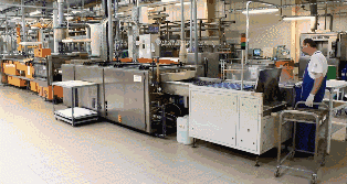
The production of PCB is very complex. Taking four-layer PCB as an example, the manufacturing process mainly includes PCB layout, core board production, inner PCB layout transfer, core board drilling and inspection, lamination, drilling, copper chemical precipitation on hole wall, outer PCB layout transfer, outer PCB etching and other steps.
1. PCB layout
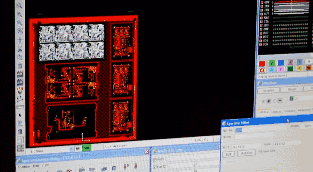
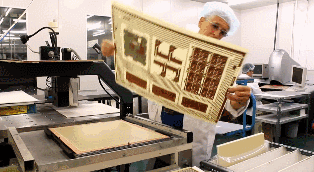
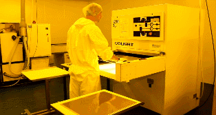
The first step of PCB production is to arrange and check the PCB layout. PCB Factory receives CAD files from PCB design company. Since each CAD software has its own unique file format, PCB Factory will convert it into a unified format — extended Gerber rs-274x or Gerber x2. Then the factory’s engineers will check whether the PCB layout conforms to the manufacturing process, whether there are any defects and other issues.
2. Manufacturing of core board
Clean the copper clad laminate, if there is dust, it may cause the final circuit short circuit or open circuit.
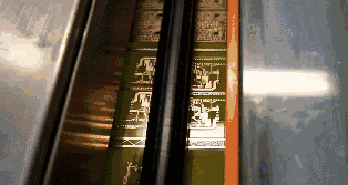
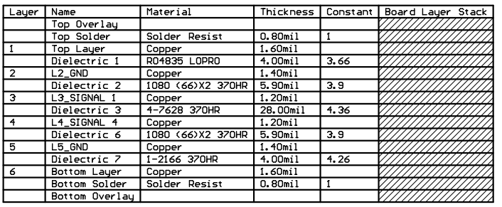
The figure below is an illustration of an 6-layer PCB, which is actually made up of three copper clad laminates (core boards) , and then bonded with PP. The production sequence is to start with the core board (3,4 layers) in the middle, continuously stack them together, and then fix them. The production of 4-layer PCB is similar, but only one core board and two copper foils are used.
3. Layout transfer of inner layer PCB
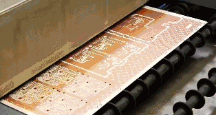
First, we need to make two layers of wiring for the core. After cleaning, the copper clad laminate will be covered with a layer of photosensitive film. The film will solidify in the light and form a protective film on the copper foil of the copper clad laminate.
The two-layer PCB layout film and double-layer copper clad laminate are inserted into the upper PCB layout film to ensure the accurate stacking position of the upper and lower layers of film.
The exposure machine uses UV lamp to irradiate the photosensitive film on the copper foil. Under the transparent film, the photosensitive film is solidified, while under the opaque film, there is no solidified photosensitive film. The copper foil covered under the solidified photosensitive film is the PCB layout circuit needed, which is equivalent to the role of laser printer ink for manual PCB.
Then clean the non cured film with alkali solution, and the required copper foil circuit will be covered by the solidified film.
The copper foil is then etched with a strong base such as NaOH.
Tear off the solidified photosensitive film to expose the required PCB layout circuit copper foil.
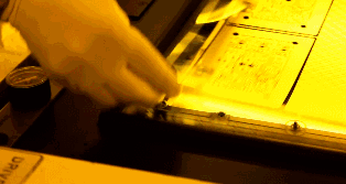
4. Core board drilling and inspection
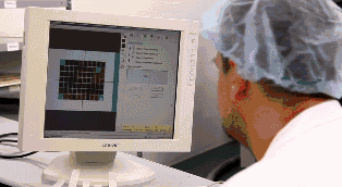
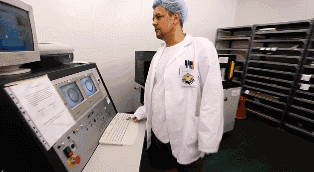
The core has been made successfully. Then, punch holes in the core plate to facilitate alignment with other raw materials. Once the core board is pressed together with other layers of PCB, it can not be modified, so the inspection is very important. The machine will automatically compare with PCB layout drawing to check the error.
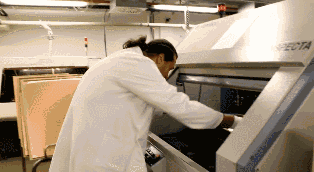
5. Lamination
The PCB boards clamped by iron boards are placed on the bracket, and then sent to the vacuum hot press for lamination. The high temperature in the vacuum press can melt the epoxy resin in PP and solidify the core board and copper foil together under pressure.
After laminating, remove the upper iron board of the pressed PCB. Then the pressure bearing steel board is taken away. The steel board also has the responsibility of isolating different PCBs and ensuring the smoothness of the outer copper foil of PCB. At this time, both sides of the PCB taken out will be covered with a layer of smooth copper foil.
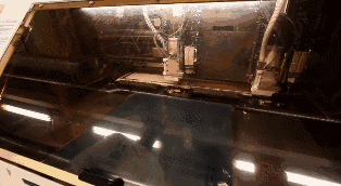
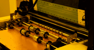
6. Drilling
Put a layer of aluminum on the punching machine, and then put the PCB on it. In order to improve the efficiency, 1 ~ 3 identical PCB boards will be stacked together to drill holes according to the number of PCB layers. Finally, cover the top PCB with a layer of aluminum plate. The upper and lower layers of aluminum plates are used to prevent the copper foil on the PCB from tearing when the drill bit is drilling and drilling out.
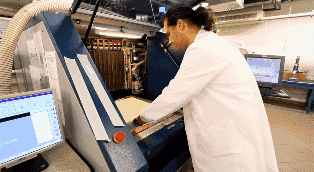
In the previous lamination process, the melted epoxy resin was extruded to the outside of the PCB, so it needs to be removed. The outline of PCB is cut by milling machine according to the correct XY coordinate.
7.PTH
8.Outer dry film
Clamp the PCB with a clamp and electroplate the copper. As mentioned earlier, in order to ensure that the hole position has enough good conductivity, the copper film on the hole wall must have a thickness of 25 μ m, so the whole system will be automatically controlled by the computer to ensure its accuracy.
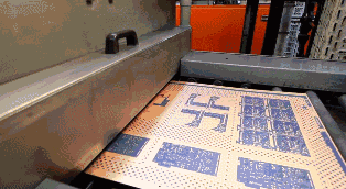
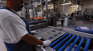
9. Outer layer etching
Next, a complete automatic assembly line is used to complete the etching process. First, the photosensitive film cured on the PCB is cleaned. Then clean the unwanted copper foil covered with it with strong alkali. Then, the tin coating on the PCB layout copper foil is removed with tin stripping solution. After cleaning, the PCB layout is completed.