Antenna module is an indispensable module in almost all communication electronic equipment. A good antenna design scheme can not only make the equipment run more stable, but also is one of the important embodiment of equipment quality.Although the antenna design seems to be a small part, it is not easy to ensure the stability of the signal. Apple mobile Iphone4S, for example, was hit by the “mobile signal gate” (cell phone signal difference) at the beginning of its listing, and a large number of iron powder make complaints about iphone4s.Although Apple later changed the design scheme to solve the problem, but from the current point of view, the Apple iPhone back design style still adopts the segmented design, whichshows that it is still very cautious in the design of the iPhone.
For the antenna design RF signal is not ideal, here are some information to share with you. Of course, the antenna design of different modules is also different. Some need to reserve T-type or π type matching circuit for antenna debugging, while others need not, which depends on the module.
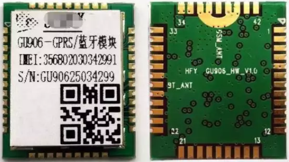
Today, the first example of case GU906 GPRS/ Bluetooth two in one module will help you understand the design of antenna PCB. I hope you can learn from today’s knowledge sharing. Antenna radio frequency parameters debugging and antenna debugging matching circuit knowledge is not repeated here, master do not spray.
Several details of GSM antenna PCB Design:
1. The antenna wiring width is 30mil
2. Shielding rules of antenna Routing: take double-sided PCB as an example, ground layer shall be laid on the bottom layer of antenna routing, and other wiring shall not be traversed or parallel; both sides of antenna routing of top layer shall be surrounded by wide and large area ground wire, and the distance between antenna wiring and stratum shall be more than 30mil.
3. The antenna wiring is regular. It is recommended that the antenna should be short and straight. It is not recommended to change layers through holes, right angle wiring and antenna length exceeding 3cm.
1. For the board level Bluetooth patch antenna, the specific PCB routing requirements are as follows: the wiring is directly from the pad pin, the wiring is recommended to be in the same plane of the module (assuming it is top), the wiring width is 15mil, the distance between the two sides from the ground is 15mil, the wiring part is required to be short, and the reference of the bottom surface is required;
2. Recommended Bluetooth Antennas: ceramic antenna, planar inverted antenna, rod antenna (2.4G frequency only). If space allows, try not to choose too small size antenna;
3. The Bluetooth antenna should be placed at the corner. If the patch antenna is selected, there should be a clearance area of at least 2mm. The clearance area should not be far away from the ground or other metal parts;
4. It is better to have a large clearance area between the antenna and the nearby objects; otherwise, the matching adjustment will be difficult and the radiation mode will be seriously distorted;
5. The lower part of the antenna should not contact the ground and ground plane;
6. The antenna should be placed away from metal objects, such as batteries, chips and other metal objects overlap.
7. Pay attention that the internal cable (such as battery power cable) is too close to the antenna;
8. Monopole antenna needs to have a reasonable ground to play the best effect.
9. There should be no metal shell or plastic with metal around the antenna.
10. Do not use very thin antenna feeders. The fixed width limit should not be less than 0.1 mm.