PCBSky
service@pcbsky.com +86-755-33583558 Ext 603
How to deal with PCB design impedance discontinuity?

How to deal with PCB design impedance discontinuity?

As PCB design engineers, we all know that impedance should be continuous. However, PCB design always has impedance can not be continuous, at this time how to do?

What is impedance

To clarify a few concepts, we often see impedance, characteristic impedance, instantaneous impedance. Strictly speaking, they are different, but they are still the basic definition of impedance
a) The input impedance at the beginning of transmission line is referred to as impedance;
b) The instantaneous impedance that the signal meets at any time is called instantaneous impedance;
c) If the transmission line has a constant instantaneous impedance, it is called the characteristic impedance of the transmission line.
Characteristic impedance describes the transient impedance of a signal propagating along a transmission line, which is a major factor affecting the signal integrity of a transmission line circuit.
If there is no special description, the characteristic impedance is generally used to call the transmission line impedance. The factors affecting the characteristic impedance are: dielectric constant, dielectric thickness, line width, copper foil thickness.

IMPEDANCE

What is impedance continuity

The impedance is continuously similar to:
The water flows steadily in a uniform ditch, and suddenly the ditch turns and widens.
Then the water will shake at the corner, and the water wave will spread.
This is the result of impedance mismatch.

Solution to impedance discontinuity

A.Gradient line

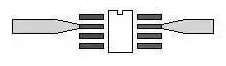
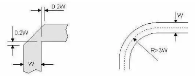
Some RF device packages are small, SMD pad width may be as small as 12mils, while RF signal linewidth may be more than 50mils, so gradient line should be used and sudden change of line width is prohibited. The gradient line is shown in the figure, and the line of transition part should not be too long.

B.Corner

If RF signal line runs at right angle, the effective line width at the corner will increase, and the impedance will be discontinuous, causing signal reflection. In order to reduce the discontinuity, there are two ways to deal with the corner: chamfering and fillet. The radius of arc angle should be large enough. Generally speaking, it should be ensured that R > 3W. As shown on the right.

C.Large pad

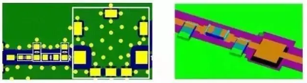
When there is a large pad on a 50 ohm thin microstrip line, the large pad is equivalent to the distributed capacitance, which destroys the characteristic impedance continuity of the microstrip line. Two methods can be used to improve the performance: firstly, the dielectric of the microstrip line is thickened; secondly, the ground plane under the pad is hollowed out, which can reduce the distributed capacitance of the pad. As shown in the figure below.

D.Via

The via hole is a metal cylinder plated outside the through hole between the top layer and the bottom layer of the circuit board. Signal vias connect transmission lines on different layers. Through hole residual pile is the unused part of through hole. Via pads are ring shaped gaskets that connect vias to top or internal transmission lines. The isolation panel is an annular space in each power or ground plane to prevent short circuit to the power supply and ground plane.

The vias are one of the important factors that cause the impedance discontinuity on RF channel. If the signal frequency is greater than 1GHz, the influence of vias should be considered.
The common methods to reduce the impedance discontinuity of the via hole are: adopting no pad process, selecting the outlet mode, optimizing the diameter of the reverse pad, etc. Optimizing the diameter of reverse pad is a common method to reduce impedance discontinuity. As the via characteristics are related to the structure size of aperture, pad, reverse pad, stack structure and outlet mode, it is suggested that HFSS and optimetrics should be used for optimization simulation in each design.
When the parametric model is adopted, the modeling process is very simple. During the review, PCB designers are required to provide corresponding simulation documents.
The diameter of via hole, pad diameter, depth and reverse pad will change, resulting in impedance discontinuity, reflection and insertion loss.

E.Through hole coaxial connector

Similar to the via hole structure, the through-hole coaxial connector also has impedance discontinuity, so the solution is the same as the via hole. The common methods to reduce the impedance discontinuity of through-hole coaxial connector are the same: adopting diskless process, appropriate outlet mode, and optimizing reverse pad diameter.

Related Articles
  • TEL:+86-755-33583558 Ext 603
  • EMAIL:service@pcbsky.com
  • ADDRESS:Add: 407, Kanglan Fortune Center, Fuzhou Avenue, Fuyong Street, Baoan District, Shenzhen, Guangdong 518103, China