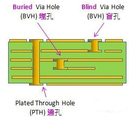
With the improvement of the performance of electronic products, PCB is constantly updated and developed. The circuit is more and more dense, and more components need to be assembled. However, the size of PCB will not become larger, but smaller and smaller. At this time, it needs considerable technology to drill holes in PCB.
There are many kinds of PCB drilling technology. The traditional method is to make inner blind holes. When Multilayer PCB is laminated step by step, two double-sided PCBs with through vias are used as the outer layer, and then laminated with the inner board without vias. The blind vias filled with glue can appear, while the blind vias on the outer board are formed by mechanical drilling. But in the production of machine drilling blind via, it is not easy to set the drill depth, and the bottom of the tapered hole affects the effect of copper plating. In addition, the production process of inner blind via is too lengthy, wasting too much cost, so the traditional method is more and more unsuitable.
Now the commonly used PCB micro via technology, in addition to the carbon dioxide drilling and laser drilling, there are mechanical drilling, photosensitive drilling, laser drilling and so on.
Mechanical drilling is made by high-speed machining, and the most important one is the drill tool. The drill tool is generally made of tungsten cobalt alloy, which is sintered by high temperature and high pressure with tungsten carbide powder as the matrix and cobalt as the binder. It has high hardness and high wear resistance, and can drill the required holes smoothly.
Laser drilling is made by cutting with CO2 and UV laser. Gas or light beam, with strong heat, can burn through the copper foil, you can make the required hole. The principle is the same as cutting, mainly controlling the beam.
Plasma, which is composed of particles with large spacing, is in an irregular continuous collision, and its thermal motion is similar to that of ordinary gas. Plasma etching is mainly used for PCB with resin copper layer. Oxygen containing gas is used as plasma. After contacting with copper, it will produce oxidation reaction, and then remove resin material to form holes.
As previously introduced in
PCB manufacturing, the objects that remain on PCB can not be cleaned by general methods. Chemical cleaning method can be used to make the chemical agent react with the residues, and then they can be removed. In the same way, the use of chemical agents, drop in the need to drill the place, you can be copper foil, resin, etc. erosion, eventually forming holes.