After PCB design, the most important step before PCB production is to export Gerber file.There are three versions of the existing Gerber file:
Gerber x2: the latest Gerber format, which can insert layer information and attributes of boards;
Extended Gerber (rs-274x) is widely used;
The standard Gerber, or rs-274d, is an old version, which is gradually being abandoned and replaced by rs-274x.
1. Output only Gerber rs274x format
Rs-274-d format has been abandoned. The current mainstream Gerber format is rs274x format. As for the latest Gerber x2 format, many PCB design software has not yet supported it, and many board manufacturers’ CAM software has not yet supported it.
2. Only positive output
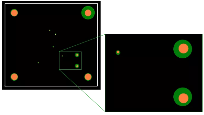
Gerber positive: what you see is what you get, that is, where there is a drawing, the copper foil of the PCB is retained, and the copper foil where there is no drawing is removed.
Gerber negative: opposite to the positive film, the copper foil of PCB is removed where there is drawing, and the copper foil is reserved where there is no drawing.
In fact, negative film is a legacy of the 1960s and 1970s, when it was still the era of vector photo plotter. Negative film was born for vector photo plotter. Vector photo plotter was the first generation photo plotter. Vector photo plotter is similar to pen plotter, but it does not use ink and paper, but uses fixed light pen to write exposure information into photographic film. The film is fixed on a platform, which can move in the plane of X-Y axis. The light pen fixed on the top of the platform irradiates the film. The light beam can be opened and closed according to the image information. Each action is controlled by commands in the entered Gerber file.Vector photo plotter is good at drawing lines, but for large area plane such as copper coating, vector light plotter will be confused. For example, when we draw with pencil, we need to fill the plane one by one, until the plane is filled gradually. When the vector photo plotter draws large plane filling, it needs to carry out a lot of movement control Film is what you see is what you get (WYSIWYG) mode, which will cause the Gerber file to contain a large number of drawing control instructions, which makes the Gerber file extremely large. Therefore, in order to solve the problem that vector photo plotter is not good at drawing and filling the plane, the negative format is generally adopted for the places where a large number of copper sheets need to be reserved in the inner layer, and the vector photo plotter only needs to draw the parts that need to be cleared This method can greatly save the work time of vector photo plotter, and the Gerber file is relatively small.
However, with the innovation of technology, photo plotter has entered the laser era, and negative film can not provide any benefits. The speed of laser photo plotter is the same for routing and large area plane filling. Therefore, all positive films are produced and what you see is what you get is convenient for cam engineers to check and confirm manually.
3. Equal rate output
Output Gerber data to
PCB manufacturer, remember to maintain 1:1 equal rate output.
4. The unit and precision of photo drawing and drilling file should be consistent
If photo drawing is output in metric units, please keep metric units when exporting drilling data. If photo drawing uses English units, please also keep English units for drilling data.
In addition, the accuracy should also be consistent. For example, the English units should be 2:5 or the metric units should be 3:3
If the photo drawing is not consistent with the drilling unit or accuracy, it may cause the deviation between the drilling hole and the center of the hole ring.
5. Do not make offset compensation
In other words, do not set offset, and keep the value of 0. If you must set offset, please keep the offset value of all Gerber files the same.