We need to check the main board device encapsulation carefully to avoid mistakes. Especially for the new materials used in the project, it is necessary to check PCB encapsulation with reference to spec.
Before wiring, we need to determine the main stratum, power layer, and roughly plan which layer the data line, IQ line, impedance line, audio line, high frequency signal line, control line and so on.
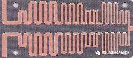
Take the common 8-layer single-stage RF part single-sided pendulum motherboard as an example. The 8th layer is for component placement, the 1st layer is not for component placement, the 6th layer is for sub ground, and the 4th layer is for main site. The power supply and data lines go through the second and third layers, and the TX and Rx impedance lines should go through the eighth layer as far as possible, and the seventh layer should be hollowed out. Refer to the sixth layer. The 7th layer shall not be wired as far as possible. IQ line, audio cable, AFC, APC, 26MHz and impedance line are easy to be interfered with. If special grounding is required, layer 5 can be used, and both upper and lower layers need to be covered with ground. The fourth floor is the main ground, and the sixth floor is the auxiliary ground. Try not to route.
4. Wiring specification
4.1 impedance line
The impedance line should go to the surface as far as possible. When going through the surface layer, the bottom layer should be hollowed out, and the next layer should be used as the reference ground. When walking through the inner layer, both the upper and lower layers need to be protected, and the left and right sides should also be well covered. The location of the 27 holes drilled, the 1st and 8th floor should be the ground. Keep away from data line, power line and signal line as far as possible. TX impedance line is controlled by 50ohm, RX impedance line is 150 ohm differential line. RX differential impedance control lines should be parallel, close and equal in length.
4.2 high frequency signal line
High frequency signal lines, such as 26MHz, edclk, etc., need special protection to avoid interference with GSM reception. Try to go inside and take the shortest distance. Both the upper and lower floors need to be covered. If 27 holes need to be drilled, make sure that the 1st and 8th layers of 27 hole positions are both ground. The high frequency signal line can not walk near the antenna area.
4.3, APC, AFC, IQ line and control line to be protected
IQ line needs special protection, and generally goes through the middle layer, such as 5 layers. The upper and lower floors need to be on the ground. The left and right sides need to be covered with copper for protection. Try to keep away from interference sources, such as power line, data line, high frequency signal line, etc. At the same time, 27 holes of the above interference sources should be avoided, too close to the IQ line. Since the IQ line is a differential line, it needs to be parallel, close and equal length. IQ line as far as possible to go straight, the shortest distance. APC and AFC need to be covered separately, and the upper and lower layers should be the ground. Keep away from interference sources. Other control lines, such as band select, PA enable of PA and band select of FEM, can go together to cover the ground as much as possible and keep away from interference sources.
4.4 power and ground
It is very important to route the power supply on the motherboard. Try to make the whole power network star type, avoid the O-type power network, form the power loop, and reduce the EMC performance. When PA works, it consumes a lot of current. In order to avoid too large voltage drop of PA input power supply, the power supply line of PA must be thick, with a general line width of 80mil. When changing the layer, more mechanical holes and laser holes should be drilled. Make it fully connected and need more holes at the connection with battery connector. The power cord of vcca and vccb pin pin pin of pasky77328 of skyworks should be pulled out from the battery connector, and the line width should be at least 16ml. The power supply to the tranceiver should also be pulled out from the battery connector separately, with a line width of 16mil.. The 26MHz crystal oscillator power supply is output from PMU, and also needs to be protected with a line width of 12mil. Other avdd, dvdd, vccrf, etc., can walk 12mil. Except for PA power supply, there should be at least 2 holes for other power lines when changing layers. All power lines are interference sources, so they should not be close to lines or devices that are susceptible to interference. Also can not be close to the high-frequency signal line, otherwise the high-frequency signal interference will be full of the whole motherboard along with the power line.
The ground of battery connector shall be fully connected with the ground of main board. As far as possible, large holes shall be drilled to the main ground to make it directly connected with the main ground. The more holes are beneficial, so as to ensure that the ground circuit of each layer of the main board can be fully formed near the battery connector. Large holes should be drilled near the power line to the main ground to make the circuit area smaller and improve the EMC performance. More small holes and large holes should be drilled at the pad of shielding frame to fully connect with the main ground. At the edge of the plate, large and small holes should be made as much as possible to improve the EMC performance. The pad under PA, FEM and transceiver is usually large and small, which is fully connected with the main ground and beneficial to PA heat dissipation. More large and small holes should be drilled under the 26MHz crystal oscillator pad.
There are also several areas where copper laying needs to be banned.
a. GSM, Bluetooth, mobile TV and other antenna break point pad, 1 to 8 layers are prohibited to lay copper. In case of monopole antenna, copper laying is forbidden in the whole antenna area from layer 1 to layer 8.
b. If the RF device is placed in the 8th layer, the ground of the 7th layer is disconnected along the shielding frame and the outer ground, and is directly connected with the main ground by the large hole.
c. The lower layer of the 26MHz crystal oscillator is also separated from the surrounding ground, and is directly connected with the main ground by the large hole.
In a word, the more holes are, the better. However, if you drill too many holes in a large area without wiring, the
PCB factory may have some opinions, which will lead to the confirmation of PCB engineering.
5 producibility check
Check whether the components in the shield cover are too close to the shield cover, which will cause short circuit. The safety distance is 12mil.
Check whether the electronic components are too close to the board edge, and the electronic components are easy to fall off.
Check the holder mask layer, antenna pad, speaker pad, receiver pad, vibration motor pad, etc. to determine whether tin is needed.
Some common network wiring precautions are attached
1. TX line is 50ohm impedance line. Adjust the line width according to the actual situation.
2. RX line is a 150 ohm differential impedance line. The line width should be adjusted according to the actual situation. Two pairs of parallel, close and equal length are required.
3. PA power supply, 80mil, need more holes when changing layers. At least 2 large holes and 4 small holes.
4. PA, vcca, vccb, need to take a single wire from the battery connector, with a line width of 16mil.
5.6129 power supply, need to separate from the battery connector, a line width of 16mil.
6, IQ line, 6mil, need to cover the ground up and down, left and right. They should be parallel, close and equal in length.
7. APC and AFC should be covered well for 4mil. Other control lines should be 4mil, covering the ground as much as possible.
8, 26MHz signal line runs 4mil, and the ground should be well covered.
9. The power lines of other radio frequency parts shall be 16 mil, and two small holes are required for layer change.
10. More grounding via holes should be drilled under FEM, PA and transceiver.