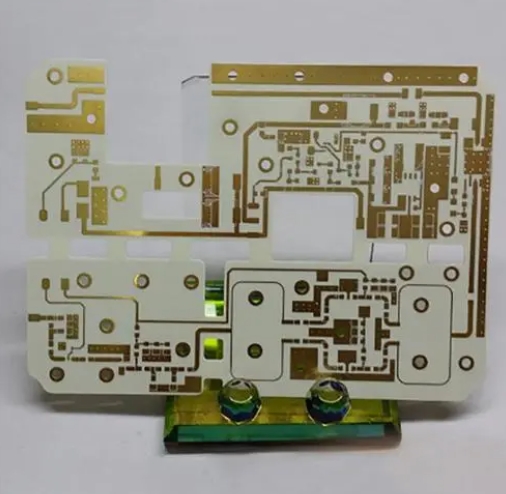
Wiring high frequency PCBs requires careful consideration of signal integrity, impedance matching, and minimizing electromagnetic interference (EMI). Here’s a practical guide to wiring high-frequency PCBs:

- Layer Stack-up:
- Choose a layer stack-up that minimizes signal losses and provides controlled impedance. Typically, high-frequency PCBs have dedicated signal layers and ground planes to manage return paths effectively.
- Impedance Control:
- Maintain controlled impedance for signal traces by using specialized PCB materials and precise trace width and spacing. Impedance calculators and simulation tools can help with this.
- Transmission Lines:
- Use transmission lines, like microstrips or striplines, for routing high-frequency signals. Proper termination and matched impedance are essential to minimize signal reflections.
- Grounding:
- Implement a solid, low-impedance ground plane to provide a stable reference plane for signals. Avoid routing signals over splits in the ground plane.
- Signal Integrity:
- Minimize signal skew and maintain signal integrity by ensuring that traces are of equal length. Differential pairs should be routed together to maintain their relative spacing.
- Avoid 90-Degree Bends:
- Sharp corners and 90-degree bends can lead to signal degradation and EMI. Use 45-degree bends or curved traces instead.
- Differential Pair Routing:
- Route high-speed differential pairs closely together with consistent spacing to maintain controlled impedance.
- Spacing and Clearance:
- Maintain adequate spacing and clearance between traces to prevent crosstalk and interference. Follow manufacturer guidelines for minimum spacing.
- Signal Return Paths:
- Ensure that the return paths for signals are as close as possible to the signal trace to minimize loop area. Avoid vias in high-frequency signal paths when possible.
- Via Placement:
- Use microvias or blind vias for layer transitions, and minimize the use of through-hole vias. Proper via placement helps reduce signal discontinuities.
- Ground Stitching Vias:
- Add ground stitching vias around high-frequency components to connect the local ground plane to the main ground plane. This reduces ground loops and improves signal quality.
- Component Placement:
- Place high-frequency components close to each other and minimize the distance between them and the connector or source. This reduces parasitic capacitance and inductance.
- Power Distribution:
- Design a clean and low-noise power distribution network. Isolate power domains and use dedicated power and ground planes for different components.
- Shielding:
- Consider adding shielding cans or enclosures for sensitive components to prevent EMI and RF interference.
- Simulation and Analysis:
- Use simulation tools and impedance analyzers to validate your high-frequency design. This helps identify and address signal integrity issues.
- Testing and Validation:
- After PCB fabrication, perform high-frequency testing, such as vector network analysis (VNA) and time-domain reflectometry (TDR), to ensure that the PCB meets design specifications.
- Document Everything:
- Keep detailed documentation of the PCB design, including materials used, trace widths, impedance values, and routing guidelines for future reference.
Designing high-frequency PCBs is a complex task that requires a deep understanding of electromagnetic principles and careful attention to detail. Following these guidelines and seeking expert advice, when needed, will help ensure the successful design and performance of your high-frequency PCBs.

