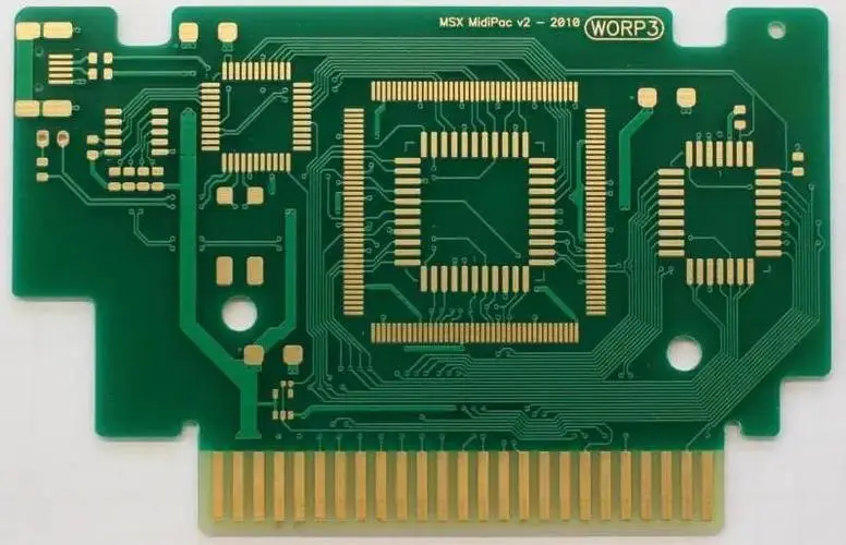
Layering and color changes in the gold-plated layer of a PCB (Printed Circuit Board) can be indicative of various issues or changes that may occur during the PCB manufacturing process or over time. Here are some reasons for layering and color changes in the gold-plated layer of a PCB:

- Oxidation: Gold is known for its resistance to corrosion and oxidation, but it is not completely immune. Over time, exposure to environmental factors such as moisture, humidity, or contaminants can lead to a layer of oxide forming on the gold surface. This oxide layer can appear as a color change and may affect the performance of the gold-plated contacts.
- Improper Handling: Goldfinger PCBs are sensitive to handling. Touching the gold-plated areas with bare hands can transfer oils, salts, and other contaminants, which may lead to discoloration and layering. Proper handling practices, including wearing gloves, can help prevent this issue.
- Contaminants: PCBs can be exposed to various contaminants during manufacturing, assembly, or use. Contaminants such as dust, chemicals, or airborne particles can settle on the gold-plated surface, causing changes in color and layering. Regular cleaning and maintenance can help mitigate this problem.
- Solder Mask or Solder Residue: During the assembly process, solder masks and soldering processes can leave residues on the gold-plated surfaces. These residues, if not cleaned properly, can lead to layering and color changes over time.
- Gold Plating Thickness: Inconsistent gold plating thickness can cause variations in color. Thicker gold plating may appear more yellow or reddish, while thinner plating may appear lighter in color. Maintaining uniform plating thickness across the board is important to avoid these variations.
- Electrochemical Migration: If the PCB is subjected to harsh environmental conditions or voltage potentials, electrochemical migration may occur. This can result in the movement of metal ions within the PCB, causing layering and discoloration over time.
- Exposure to UV Light: Prolonged exposure to ultraviolet (UV) light, especially in outdoor or high-intensity UV environments, can lead to color changes in the gold-plated layer. UV light can cause photochemical reactions with the gold surface, altering its color.
- Chemical Exposure: Exposure to harsh chemicals or cleaning agents can erode the gold plating, leading to discoloration and layering. Proper cleaning methods that do not harm the gold layer are essential.
- Aging: Over time, gold plating may naturally age, leading to color changes. This aging can be accelerated by factors such as temperature fluctuations, humidity, and environmental conditions.
To prevent and address these issues, it is essential to follow best practices for PCB handling and storage, use appropriate cleaning methods, and ensure that the manufacturing and assembly processes adhere to industry standards. Regular inspection and maintenance of PCBs can help detect and address discoloration and layering early to maintain optimal performance and reliability.

