PCB board design needs to provide information:
(1) Schematic diagram: a complete electronic document format, which can generate correct netlist;
(2) Mechanical size: provide the specific position and direction identification of positioning device, as well as the identification of specific height limit position area;
(3) BOM list: it mainly determines and checks the specified package information of equipment on the schematic diagram;
(4) Wiring Guide: description of specific signal specific requirements, as well as design requirements for impedance, lamination, etc.
The basic design process of PCB design is as follows:
Preparation > PCB structure design >
PCB layout > wiring > wiring optimization and screen > network and DRC check and structure check > PCB board.
1: Preliminary preparation
1) This includes preparing component libraries and schematic diagrams. “If you want to do something good, you have to hone your tools first.” In order to build a good board, in addition to the design principles, you have to draw well. Before proceeding with PCB design, you must first prepare the component library of schematic Sch and the component library of PCB (this is the first step – very important). Component libraries can use libraries that come with Protel, but it’s often difficult to find the right library. It is better to complete the component library according to the standard size data of the selected equipment.
In principle, first execute the component library of PCB, and then execute the component library of sch. PCB component library has higher requirements, which directly affects the circuit board installation; Sch component library requirements are relatively loose, as long as you pay attention to the definition of pin attributes and the corresponding relationship with PCB components.
PS: pay attention to the hidden pin in the standard library. Then there is the schematic design. When it is ready, you can start PCB design.
2) When making a schematic library, pay attention to whether the pins are connected to the output / output PCB board and check the library.
2. PCB structure design
This step draws the PCB surface in PCB design environment according to the determined board size and various mechanical positioning, and places the required connector, button / switch, nixie tube, indicator, input, and outputs according to the positioning requirements. For example, the scope of screw hole is non wiring area.
Special attention should be paid to the actual size (occupied area and height) of components, the relative position between components – the size of space, and the surface on which the equipment is placed to ensure the electrical performance of the circuit board. In the production and installation of the feasibility and convenience at the same time, to ensure that the above principles can be reflected, the equipment should be appropriately modified to make it clean. If the same device is placed neatly and in the same direction, it cannot be placed. This is a patchwork. “
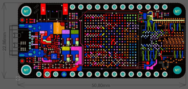
3. PCB layout
1) Make sure the pre layout schematic is correct – this is very important! —– very important!
The schematic diagram has been completed and the inspection items are: power grid, ground grid, etc.
2) The layout should pay attention to the surface equipment (especially plug-ins, etc.) and the placement mode (plug-in horizontal or vertical) to ensure the feasibility and convenience of installation.
3) The layout is white and the device is placed on the circuit board. At this point, if all the above preparations are completed, you can generate the network table (Design > create netlist) on the schematic diagram, and then import the network table (Design > loadnets) on the PCB. I see the complete device stack, and there are flying wires between the pins to indicate the connection, and then the device layout can be carried out.
The overall layout is based on the following principles:
When I lie down in the layout, you should determine the surface on which to place the device: in general, patches should be placed on the same side, and plug-ins should check for details.
1) According to the reasonable division of electrical performance, it is generally divided into: digital circuit area (interference, interference), analog circuit area (afraid of interference), power drive area (interference source);
2) Circuits with the same function should be placed as close as possible, and the components should be adjusted to ensure the simplest connection; at the same time, the relative position between function blocks should be adjusted to make the connection between function blocks the most concise;
3) For high-quality components, the installation position and strength should be considered; the heating elements should be placed separately from the temperature sensitive elements, and the thermal convection measures should be considered when necessary;
4) The clock generator (such as crystal or clock) should be as close as possible to the equipment using the clock;
5) Layout requirements should be balanced, sparse and orderly, not top heavy or sink.
4. Wiring
Wiring is the most important process in PCB design. This will directly affect the performance of PCB. In the process of PCB design, there are three levels of wiring: the first is connection, and then is the most basic requirement of PCB design. If the line is not laid and the line is flying, it will be a disqualified board. It hasn’t started yet, so to speak. The second is the satisfaction of electrical performance. This is an index to measure the qualification of printed circuit boards. This is after connection, carefully adjust the wiring to achieve the best electrical performance, followed by aesthetics. If your wiring is connected, then there is no place to affect the performance of electrical appliances, but in the past, there are many bright colors and rich colors. How good your electrical performance is, in other people’s eyes, is still a piece of garbage. This brings great inconvenience to testing and maintenance. Wiring should be neat and even without rules and regulations. These must be achieved while ensuring electrical performance and meeting other personalized requirements.
5. Add tears
Tear drop is the drip connection between pad and line or between line and guide hole. The purpose of tear drop setting is to avoid the contact point between wire and pad or between wire and guide hole when circuit board is subjected to large external force. In addition, disconnection and tear drop setting can make PCB look more beautiful.
In the circuit board design, in order to make the pad stronger and prevent the fracture between the pad and the welding wire when making the mechanical board, the copper film with transition zone is usually set between the pad and the welding wire, which is shaped like tears, so it is usually called tear drop.
6. Conversely, the first check is to look at the keepout layer, the top layer, the bottom layer, the top overlay and the bottom overlay.
7. Inspection of electrical rules: through hole (0 through hole – very inconceivable; 0.8 boundary line), whether there is a disconnected network list, minimum spacing (10mil), short circuit (each parameter is analyzed one by one)
8. Power line and ground wire check – interference. (filter capacitor should be close to chip)
9. After completing the PCB, reload the network tag to check if the netlist has been modified – it works properly.
10. After the PCB is completed, check the circuit of the core equipment to ensure the accuracy.