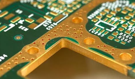
What is the function and principle of grounding via hole near the wiring via hole?
According to their functions, the through holes of
PCB board can be divided into the following categories:
1. Signal vias (via structure requirements have the least impact on signals);
2. Power and ground vias (via structure requires minimum distributed inductance of vias);
3. Thermal vias with minimum thermal resistance.
The vias mentioned above belong to grounding type vias. The function of adding grounding via holes near via holes is to provide a shortest return path for signals. Note: the through-hole of the signal layer changing is an impedance discontinuity point, and the return path of the signal will be disconnected from here. In order to reduce the area surrounded by the signal return path, some ground vias must be drilled around the signal via to provide the shortest signal return path and reduce the EMI radiation of the signal. The radiation increases with the increase of signal frequency.
Under what circumstances should more grounding vias be drilled?
There is a saying: drilling more holes will destroy the continuity and integrity of the formation. The effect is counterproductive.
First of all, if more holes are drilled, resulting in the continuity and integrity of the power layer and stratum, this situation should be avoided. These vias will affect the integrity of the power supply, resulting in signal integrity problems, great harm. Hole drilling usually occurs in the following three situations:
1. Grounding vias are used for heat dissipation;
2. Grounding vias are used to connect multi-layer plates;
3. Grounding vias are used for the location of vias for layer changing of high-speed signals.

