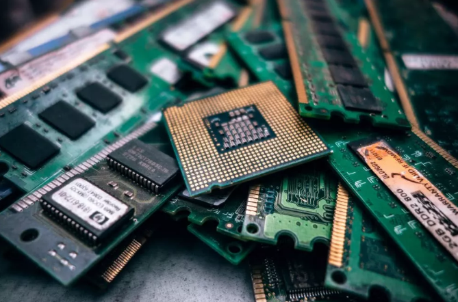
There are single-sided, double-sided and multi-layer PCB boards. The number of layers of multi-layer PCB is unlimited. At present, there are more than 100 layers of PCB, while the common multi-layer PCB is four-layer and six-layer PCB. Then why do you have “Why are multilayer PCB boards even?” What about this question? Relatively speaking, even layer PCB is more than odd layer PCB, and has more advantages.
1. Low cost
Because of the lack of a layer of medium and copper foil, the raw material cost of odd PCB is slightly lower than that of even PCB. However, the processing cost of odd layer PCB is significantly higher than that of even layer PCB. The processing cost of the inner layer is the same, but the copper foil / core structure obviously increases the processing cost of the outer layer.
Odd layer PCB needs to add non-standard lamination core bonding process on the basis of core structure technology. Compared with the nuclear structure, the production efficiency of the factory with foil coating outside the nuclear structure will be reduced. Prior to lamination bonding, the outer core requires additional processing, which increases the risk of scratches and etching errors on the outer layer.
2. Balanced structure to avoid bending
The best reason not to design PCB with odd layers is that odd layers are easy to bend. When the PCB is cooled after the multilayer circuit bonding process, the different laminating tension between the core structure and the copper foil structure will cause PCB bending. With the increase of PCB thickness, the bending risk of composite PCB with two different structures increases. The key to eliminate PCB bending is to use balanced stacking. Although a certain degree of bending PCB meets the specification requirements, the subsequent processing efficiency will be reduced and the cost will be increased. Because special equipment and process are needed during assembly, the placement accuracy of components is reduced, so the quality will be damaged.
In other words, it is easier to understand: in PCB process, four layer PCB is better than three-layer PCB, mainly in symmetry. The warpage of four-layer PCB can be controlled below 0.7% (ipc600 standard). However, when the size of three-layer PCB is large, the warpage will exceed this standard, which will affect the reliability of SMT chip and the whole product, so the general designers do not set it Even if the function of odd layer PCB is realized, it will be designed as false even layer, that is, 5 layers are designed as 6 layers and 7 layers as 8 layers.
Based on the above reasons, the multi-layer PCB board is mostly designed as even layer, and the odd number layer is less.