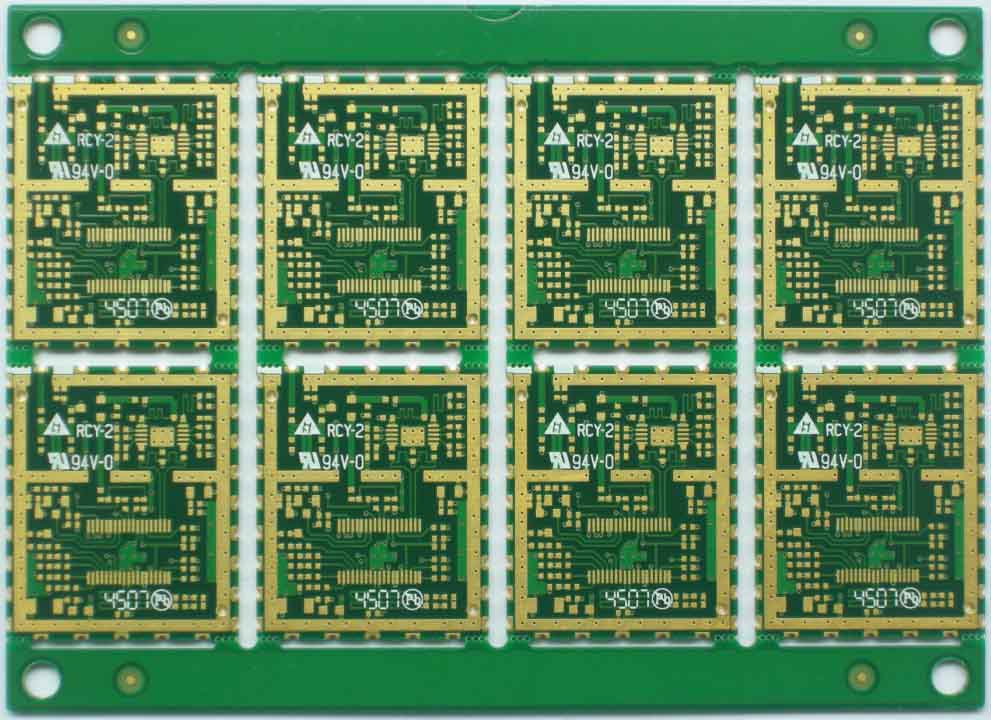
A “half hole” in the context of printed circuit boards (PCBs) refers to a type of plated through-hole (PTH) that does not extend through the entire thickness of the PCB substrate. Instead, it only goes partially through the board, leaving a hole with a depth that is less than the full thickness of the PCB. These half holes are also known as castellated holes.

Half holes are commonly used in PCBs for various purposes, including:
The design and implementation of half holes in a PCB involve careful consideration of their size, spacing, and location to ensure compatibility with the components or connectors that will be attached. Additionally, the process of creating half holes during PCB manufacturing involves routing or drilling holes and then plating the exposed edges with conductive material, typically copper, to ensure electrical connectivity.
Half holes are a versatile feature in PCB design, particularly when you need to combine surface-mount and through-hole components or when you require specific edge connections in your electronic devices or systems.
In production, sometimes meet some customers, require part of the hole plug hole, but can not be fully stuffed, plug hole back welding window opening, and depth requirements, commonly known as “PCB half hole“. It is understood that such customers are testing in these holes, and will punch the test probe into the hole. If there is too much ink in the hole or the hole wall is polluted by ink, it is easy to cause false opening and affect the test results. If the amount of ink in the plug hole is too small, or if the plug hole is not plugged, it can not meet the requirements of the plug hole.
Therefore, in the production process, we must control the depth of the plug hole and make the plug hole according to the depth required by customers. From the experience of conventional green plug hole, we know that the difficulty of controlling the depth of plug hole is not insufficient plug, but the accuracy of a relatively small plug hole depth and specified plug hole depth. At present, there are two main methods: one is to fill the hole or a certain depth, and then the back of the plug hole is not exposed, and some ink is washed out by developing, so as to achieve a certain plug depth effect; Second, the depth of the plug hole is strictly controlled, and then both sides of the plug hole are exposed.
The first method achieves plug hole depth control by developing and flushing part of the ink in the hole. Its advantages are simple process and easy operation. The disadvantage is that ink often pollutes the surface of the board during developing. Depth is affected by development parameters. In production, it is difficult to reach the optimal value at the same time because of considering not only the control depth, but also other conditions of panel development. In addition, the uniformity is relatively poor. The second method has a long process and relatively complex production. In batch production, the first board is needed to confirm whether the depth is appropriate, but there is no need to worry about the contamination of the panel after development.
Two methods are used to make ink shape diagrams in plug holes. It can be seen that the direct plug hole control at the same depth exposes more copper, which is conducive to customer testing. In production, the author believes that two production methods should be selected according to the production output, and adjusted appropriately to save costs and improve production efficiency.