Welcome to the ultimate guide to professional PCB design services! Whether you’re a seasoned electronic engineer or a budding entrepreneur with a brilliant product idea, mastering the art of PCB design is essential to bring your innovation to life. And that’s where professional PCB design services come in.
In this comprehensive guide, we’ll unlock the secrets of PCB design, delving into all the crucial aspects you need to know. From understanding the basics of PCB layout and component placement to navigating the intricacies of signal integrity and power distribution, we’ve got you covered.
Our brand is dedicated to providing you with valuable insights and actionable tips to optimize your PCB design process. We believe in a user-centric approach, always focusing on delivering the highest quality articles that meet your exact needs and exceed your expectations.
So, whether you’re looking for tips to enhance your PCB designs or seeking recommendations for choosing the right professional PCB design service provider, keep reading. Get ready to unlock the secrets and elevate your PCB design game to new heights!
Professional PCB design services play a pivotal role in transforming your concept into a functional and reliable printed circuit board. While some may attempt to design their PCBs in-house, partnering with professionals offers numerous advantages. These services bring expertise, experience, and access to cutting-edge tools that can save you time, money, and headaches.
One of the primary benefits of professional PCB design services is the assurance of high-quality designs. These experts have extensive knowledge of industry best practices, ensuring that your PCB meets all the necessary requirements for functionality, manufacturability, and reliability. They understand the nuances of component placement, trace routing, and design optimization to create a PCB that performs flawlessly.
Additionally, professional PCB design services provide access to advanced tools and software that streamline the design process. These tools enable faster prototyping, efficient collaboration, and comprehensive design analysis, resulting in shorter development cycles and improved time-to-market for your products. By leveraging their expertise and resources, you can focus on other critical aspects of your project while leaving the intricate details of PCB design to the professionals.
Partnering with professional PCB design services also offers scalability. As your project evolves and demands grow, these services can accommodate your changing needs. They have the flexibility to handle complex designs, multi-layer boards, and high-speed requirements. This scalability ensures that your PCB design aligns with your future goals and can adapt to the ever-changing technological landscape.
In conclusion, professional PCB design services bring expertise, access to advanced tools, scalability, and the assurance of high-quality designs. By leveraging their services, you can optimize your PCB design process and achieve exceptional results.
Professional PCB design services encompass a wide range of offerings tailored to meet various project requirements. Understanding the different types of services available can help you choose the right provider for your specific needs.
1. Full-Service PCB Design: Full-service PCB design providers offer end-to-end solutions, starting from conceptualization to final production. They handle every aspect of the design process, including schematic capture, component selection, layout design, prototype fabrication, and testing. This comprehensive approach ensures a seamless transition from design to manufacturing, saving you time and effort.
2. Layout-Only Services: If you already have a schematic and component list, layout-only services focus solely on translating your design into a physical layout. These providers specialize in PCB layout and optimization, ensuring that your design meets all the necessary criteria for functionality, manufacturability, and signal integrity.
3. Design Review and Validation: Design review and validation services evaluate your existing PCB design for potential issues and provide recommendations for improvement. They conduct thorough inspections, checking for design errors, signal integrity issues, and manufacturability constraints. These services help identify and rectify any design flaws before moving forward, saving you from costly mistakes.
4. Embedded System Design: For projects involving complex embedded systems, some PCB design services offer expertise in integrating hardware and software components. These providers specialize in creating PCB designs that seamlessly integrate with software platforms, enabling optimal performance and functionality.
Choosing the right type of professional PCB design service depends on your project’s scope, complexity, and your specific needs. Consider the stage of your project, your level of expertise, and the resources available to determine the most suitable service provider.
Selecting the right PCB design service provider is crucial for the success of your project. Here are some key factors to consider when making your decision:
1. Experience and Expertise: Look for providers with a proven track record and extensive experience in PCB design. Consider their expertise in your specific industry or application domain. A knowledgeable provider will understand the unique challenges and requirements associated with your project.
2. Technical Capabilities: Assess the provider’s technical capabilities, including their proficiency in using the latest design tools and software. Ensure they can handle the complexities of your design, such as high-speed PCBs, multi-layer boards, or specific manufacturing requirements.
3. Portfolio and Client References: Review the provider’s portfolio to gauge the quality of their previous work. Look for projects similar to yours and assess the performance and reliability of the PCBs they have designed. Client references and testimonials can also provide insights into their professionalism, communication, and overall satisfaction.
4. Collaboration and Communication: Effective communication and collaboration are vital for a successful partnership. Evaluate the provider’s communication channels, responsiveness, and willingness to understand your requirements. A transparent and collaborative approach ensures that your vision is accurately translated into the final PCB design.
5. Cost and Timelines: While cost should not be the sole deciding factor, it is essential to consider your budget constraints. Request detailed quotes from potential providers and evaluate the value they offer in relation to their pricing. Additionally, discuss project timelines to ensure they align with your expectations and deadlines.
By considering these factors, you can make an informed decision when choosing a professional PCB design service provider. Remember, this partnership will significantly impact the success of your project, so take the time to evaluate your options thoroughly.
The PCB design process involves several stages, each crucial for creating a high-quality and functional PCB. Let’s explore the key steps involved:
1. Requirements Gathering: The first step is to gather the project requirements, including functional specifications, performance criteria, and any specific constraints. This information serves as the foundation for the entire design process and helps guide subsequent decisions.
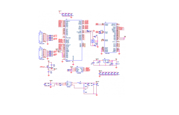
2. Schematic Capture: In this step, the circuit schematic is created using specialized software. The schematic captures the electronic connections between components, allowing for a visual representation of the circuit’s functionality.
3. Component Selection: Selecting the right components is critical for a successful PCB design. Factors such as cost, availability, performance, and compatibility with other components must be considered. Collaborate with your design service provider or consult industry experts to ensure optimal component selection.
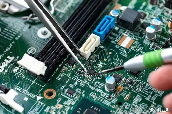
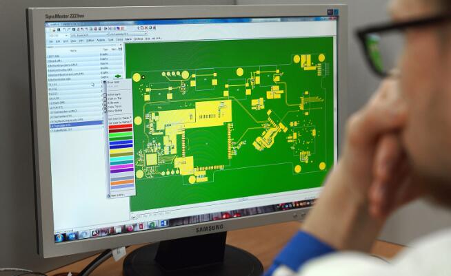
4. PCB Layout Design: The PCB layout design involves translating the schematic into a physical layout. This step includes component placement, trace routing, and layer stackup configuration. The layout design must consider factors such as signal integrity, power distribution, thermal management, and manufacturability.
5. Design Verification: Design verification is crucial to ensure the functionality and reliability of the PCB. It involves simulations, testing, and analysis to validate the design against the project requirements. Various techniques, such as signal integrity analysis, thermal analysis, and Design for Manufacturing (DFM) checks, are employed to identify and address any potential issues.
6. Prototype Fabrication: Once the design is verified, a prototype PCB is fabricated. This step involves manufacturing the PCB based on the design specifications. The prototype serves as a tangible representation of the final product and allows for further testing and validation.
7. Testing and Iteration: The fabricated prototype undergoes rigorous testing to validate its performance and functionality. Any issues or improvements identified during testing are addressed, and the design is iterated upon until all requirements are met.
8. Manufacturing and Production: After the design has been finalized and tested, the PCB design files are sent for production. Collaborate with your design service provider to ensure a smooth transition from prototype to mass production. Consider factors such as batch size, lead times, and manufacturing capabilities.
By following these steps, you can ensure a systematic and efficient PCB design process. Collaborating with professional PCB design services can streamline these steps and optimize the overall design cycle.
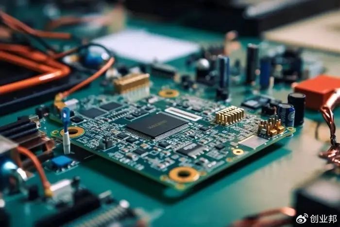
A professional PCB design consists of several key components that work together to ensure optimal performance and reliability. Let’s explore these components:
1. Schematic: The schematic serves as the blueprint of the circuit and represents the logical connections between components. It is crucial for understanding the circuit’s functionality and for subsequent stages of the design process.
2. Component Library: The component library contains a comprehensive collection of components used in the design. It includes footprints, symbols, and associated data that aid in accurate component placement and layout design.
3. Placement and Routing: Component placement involves arranging the components on the PCB in an optimal manner. It considers factors such as signal integrity, power distribution, thermal management, and manufacturability. Routing involves creating pathways (traces) on the PCB to connect the components and ensure proper signal flow.
4. Power and Ground Planes: Power and ground planes are dedicated layers on the PCB that provide stable power distribution and return paths for signals. These planes help reduce noise, minimize electromagnetic interference (EMI), and ensure proper signal integrity.
5. Decoupling Capacitors: Decoupling capacitors are strategically placed on the PCB to provide local energy storage and stabilize power supply voltages. They help reduce noise and voltage fluctuations, ensuring consistent and reliable operation of the circuit.
6. Signal Integrity Features: Signal integrity features, such as controlled impedance traces, differential pairs, and high-speed design techniques, are essential for maintaining signal integrity in high-frequency and high-speed PCB designs. These features minimize signal degradation, reflections, and crosstalk.
7. Thermal Management: Thermal management is crucial for preventing excessive heat buildup on the PCB. Proper heat dissipation techniques, such as heat sinks, thermal vias, and copper pours, ensure that components operate within their specified temperature ranges and prolong their lifespan.
By understanding these key components, you can appreciate the intricate details involved in professional PCB design. Each component plays a vital role in ensuring the functionality, reliability, and manufacturability of the final PCB.
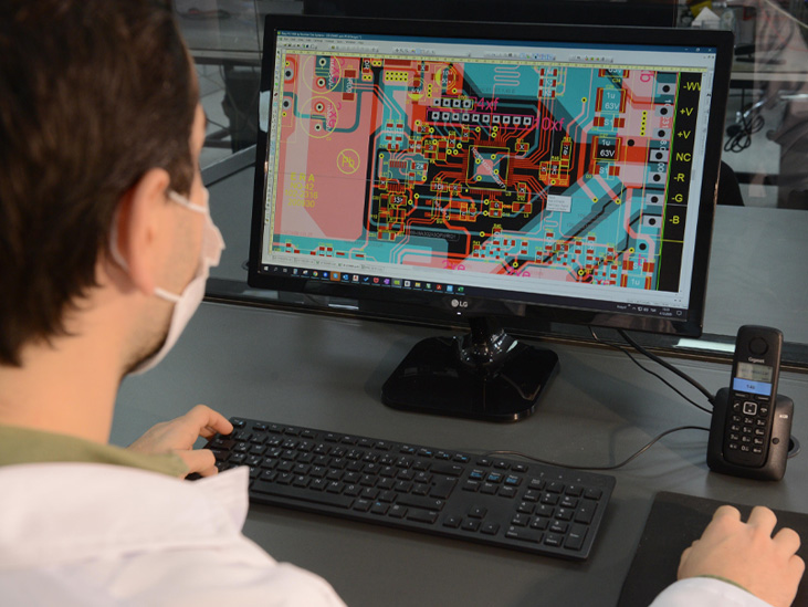
Professional PCB design services rely on a range of tools and software to streamline the design process and ensure high-quality results. Let’s explore some of the commonly used tools:
1. EDA Software: Electronic Design Automation (EDA) software is the backbone of PCB design. These software tools offer features for schematic capture, layout design, and design analysis. Popular EDA tools include Altium Designer, Cadence Allegro, and Mentor Graphics PADS.
2. Simulation Tools: Simulation tools enable analysis and validation of the PCB design before fabrication. They provide insights into signal integrity, thermal performance, electromagnetic compatibility (EMC), and other critical parameters. Popular simulation tools include SPICE, ANSYS, and HyperLynx.
3. CAD Tools: Computer-Aided Design (CAD) tools are used for creating precise and detailed 3D models of the PCB. These tools aid in component placement, mechanical integration, and design verification. Popular CAD tools include SOLIDWORKS PCB, Autodesk EAGLE, and AutoCAD.
4. Design Rule Checkers: Design Rule Checkers (DRC) ensure that the design adheres to specific manufacturing and industry standards. DRC tools automatically identify potential design errors, such as clearance violations, trace width violations, and other rule violations.
5. Collaboration and Version Control: Collaboration and version control tools facilitate efficient collaboration between team members and ensure proper management of design revisions. These tools enable multiple designers to work on the same project simultaneously, simplifying design iterations and reducing errors.
6. Manufacturing Software: Manufacturing software helps streamline the transition from design to production. It includes features for generating manufacturing files, panelization, bill of materials (BOM) management, and design for manufacturing (DFM) analysis.
Professional PCB design services leverage these tools and software to enhance productivity, accuracy, and collaboration. By utilizing the right combination of tools, they can optimize the design process and deliver high-quality PCB designs.
PCB design is a complex process that involves numerous challenges. However, professional PCB design services have the expertise and experience to overcome these challenges effectively. Let’s explore some common challenges and the strategies professionals employ to address them:
1. Signal Integrity: Maintaining signal integrity in high-frequency and high-speed designs is a significant challenge. Professionals leverage techniques such as controlled impedance routing, differential pair routing, and proper grounding practices to minimize signal degradation, reflections, and crosstalk.
2. Power Distribution: Proper power distribution is crucial for ensuring stable and reliable operation of the PCB. Professionals employ techniques such as power plane design, decoupling capacitor placement, and power integrity analysis to optimize power distribution and minimize noise.
3. Thermal Management: Effective thermal management is essential for preventing excessive heat buildup, which can degrade component performance and reliability. Professionals use techniques such as thermal vias, heat sinks, and proper component placement to ensure optimal heat dissipation.
4. Design for Manufacturability: Designing for manufacturability is critical to ensure that the PCB can be efficiently and cost-effectively manufactured. Professionals consider factors such as panelization, component footprints, solder mask design, and assembly constraints to minimize manufacturing issues and optimize yield.
5. Component Sourcing and Availability: Finding the right components and ensuring their availability can be challenging, especially for niche or specialized projects. Professionals have established relationships with component suppliers and can assist in sourcing reliable and suitable components for your design.
6. Design Verification and Validation: Validating the design against project requirements and industry standards is crucial. Professionals employ a range of simulation and analysis tools to verify the design’s performance, mitigate risks, and identify potential issues before fabrication.
By leveraging their expertise, experience, and access to advanced tools, professional PCB design services can effectively tackle these challenges. Their in-depth knowledge and industry best practices ensure that your PCB design is optimized for functionality, reliability, and manufacturability.
The cost of professional PCB design services can vary depending on various factors. Understanding these cost considerations can help you plan your budget effectively. Here are some key
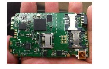
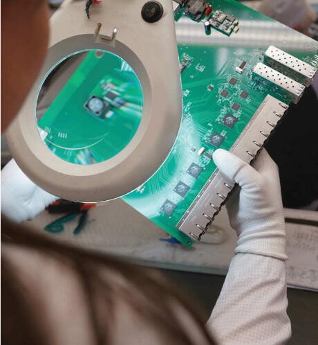
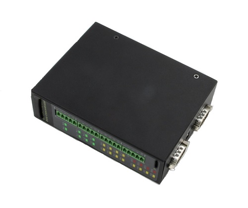
PCB layout and component placement are critical elements in designing a PCB that meets the requirements for functionality, reliability, and manufacturability. The layout of a PCB refers to the arrangement of components, traces, and other elements on the board. Component placement, on the other hand, involves positioning the electronic components on the PCB.
A well-designed PCB layout should ensure that the board is compact, easy to manufacture, and has optimal signal integrity. This can be achieved by considering factors such as the size and shape of the board, the number and type of components, and the placement of connectors and other interfaces.
When it comes to component placement, the goal is to ensure that the components are positioned in a way that optimizes functionality, reliability, and manufacturability. Some of the key factors to consider when placing components on a PCB include the size and shape of the components, their orientation, and their proximity to other components.
In addition, it’s important to consider the thermal properties of the components and the board. This involves ensuring that components that generate heat are placed in a way that allows for efficient dissipation of heat. Proper PCB layout and component placement are essential for ensuring that the PCB performs optimally and can be manufactured efficiently.
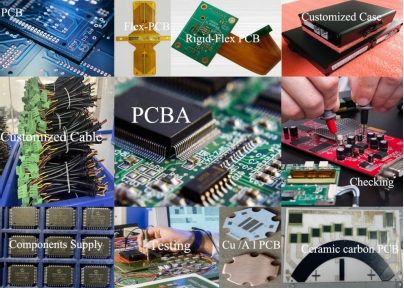
PCBSky has been in the PCB design business since 2013. We specialize in high-speed PCB design, SI/PI/EMC analysis in addition to training and consulting. With our outstanding expertise at PCB design, we offer high-quality service for over 5,000 clients all over the world. We are the largest PCB design center in China with over 600 professional engineers.
●600+ full-time professional engineers
●10000+ PCB design projects per year
●Recognized by 5000+ clients

No design, no soul! In order to produce exquisite products, the PCB design team has 5 years of PCB design and SMT engineering experience on average, providing PCB design, PCB layout and other services. It has profound PCB design experience in the field of electronic products and communication, and has been working continuously for 8 years with the speed of delivering no less than 3 finished products every day!
Product introduction:
PCBSky provides sample production and manufacturing for customers, and after the customer’s smooth acceptance, batch production is from PCBSky to a professional factory with ISO13485 qualification to produce, and PCBSky provides continuous iterative improvement service.
FAQs
1. The product always has a variety of small problems, how to keep changing?