
Thick copper board requires special copper surface and thick copper surface, so there is a great height difference between copper surface and PP substrate. For example, if uniform filling and anti-welding between lines is required, poor process control will lead to bad phenomena such as ink floatation, false copper exposure or ink unevenness. In this paper, through the test of line mask printing area, screen opening size, printing static time and printing mode, the problems of welding resistance printing of thick copper board such as false copper exposure, uneven ink, bubbles and so on were improved, and the yield of welding resistance printing of thick copper board was improved.
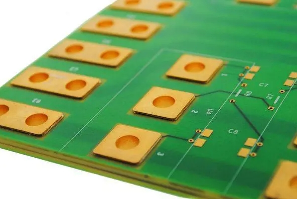
In recent years, the continuous development and maturity of consumer electronics market has also brought fierce competition to PCB manufacturers. In this case, on the one hand, PCB manufacturers (pcb manufacturing factories) have been looking for new profit points. On the other hand, PCB manufacturers constantly change the product form of OEM in order to reduce production costs. Heavy copper board, a product produced by only a few PCB manufacturers, has become the focus of 6oz copper PCB manufacturers because of its high unit price. In general, the circuit boards with copper thickness (> 2OZ) in the inner and outer layers are called thick copper boards. The main characteristics of thick copper boards are: large current carrying capacity, reducing thermal strain and heat dissipation; they are mainly used in communication equipment, aerospace, plane transformer and power supply module, etc. Thick copper board requires special copper surface, and copper thickness is thicker than that of common circuit board. Therefore, there is a great height difference between 6oz copper PCB and PP substrate. For example, it is a great challenge for the operation mode of anti-welding printing to fill the copper surface and the line evenly. If the process is not well controlled or the printing workers are not skilled enough, it will lead to the bad phenomena of ink floating, false copper exposure or ink unequal.
The process of 6oz copper PCB solder resistance printing is as follows:
pretreatment of welding resistance → weld resistance printing (using 80-150ml ink-water ink) → static 2-3H → pre drying → test → exposure → development → test → solder resist solidification → pretreatment of welding resistance (without abrasion brush) → overprint (using 80-130ml oil-water ink) → Static 2H → pre drying → test → exposure → development → test → solidification.


