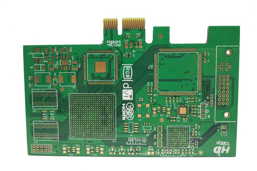
Hard gold plating PCB, also known as selective gold plating or gold plating, is a process of electroplating a layer of nickel and then a layer of gold on the required PCB pads. It is called selective because it only applies to some of the PCB pads that need it, such as edge connectors or keypads. It is also called hard gold because it is hard and wear-resistant, making it suitable for repeated abrasion.
In this article, we will introduce the manufacturing flow of hard gold plating PCB and explain why you should choose this surface finish for your PCB design.
Steps of Hard Gold Plating PCB
The manufacturing flow of hard gold plating PCB consists of the following steps:
- Drilling: The first step is to drill the holes for the vias and components on the PCB. The vertical edges of the edge connectors are also routed at this stage to align them with the printed image.
- Plating: The next step is to plate the copper on the holes and the surface of the PCB. This forms the electrical connection between the layers and the pads.
- Etching: The etching process removes the unwanted copper from the PCB, leaving only the traces and pads.
- Solder mask: The solder mask is applied on the PCB to protect it from oxidation and short circuits. The solder mask also defines the areas that need hard gold plating, such as edge connectors or keypads.
- Hard gold plating: The hard gold plating process involves electroplating a layer of nickel and then a layer of gold on the exposed pads. The nickel layer acts as a barrier between the copper and the gold, preventing corrosion and improving adhesion. The gold layer provides excellent conductivity and durability. The typical thickness of hard gold plating is 3-50 microns for nickel and 1-2 microns for gold.
- Surface finish: The final step is to apply the surface finish to the rest of the PCB. Hard gold plating is compatible with all kinds of surface finishes, such as HASL, ENIG, OSP, etc.
Advantages of Hard Gold Plating PCB
Hard gold plating PCB has many advantages over other surface finishes, such as:
- High reliability: Hard gold plating provides a reliable electrical contact that can withstand high temperatures, humidity, and corrosion. It also has a long shelf life and does not degrade over time.
- High durability: Hard gold plating is hard and wear-resistant, making it ideal for applications that require frequent insertion and removal or mechanical stress, such as edge connectors or keypads.
- High performance: Hard gold plating has low contact resistance and high conductivity, ensuring a fast and stable signal transmission. It also has low solderability, which prevents solder bridging and short circuits.
Conclusion
Hard gold plating PCB is a popular surface finish for PCBs that need high reliability, durability, and performance. It is especially suitable for edge connectors or keypads that require repeated abrasion. If you are looking for a professional PCB manufacturer that can provide high-quality hard gold plating PCBs, you can trust PCBSky. PCBSky is a leading PCB manufacturer in China that offers various types of PCBs with different surface finishes at competitive prices. Contact us today to get a free quote for your hard gold plating PCB project.
Hard gold plating PCB has excellent electrical conductivity, wear resistance, oxidation resistance and reduced contact resistance. But gold is extremely expensive, so it is only used for topical gold plating or chemical gold on goldfinger.
Hard gold plating PCB production process: upper – grinding plate (micro erosion) – washing, activation, washing, nickel plating, washing, activation, washing, gold plated, gold recovery – water – air drying – the lower.
Hard gold plating PCB steps: adhesive tape — roller tape — automatic nickel-gold plating — tape tearing — washing and drying.


