Polytetrafluoroethylene is referred to as PTFE, which has a wide range of use temperature, excellent chemical stability, electrical insulation, self-lubricating, aging resistance and other excellent properties. It is widely used in many fields. However, the application of polytetrafluoroethylene in device manufacturing often encounters problems related to its surface properties. Poor surface wettability can lead to adhesion problems, not only for adhesives, but also for inks, coatings and biomaterials.
What is plasma?
Plasma is a state of matter, just like a solid, liquid or gas. Add enough energy to the gas and the gas will ionize into a plasma. Chemically, it is a highly reactive environment for changing surface properties without affecting bulk materials. Gas plasma treatment is a powerful tool to solve the problem of surface treatment. It provides a reliable, consistent and environmentally friendly nano scale cleaning and activation method to improve surface wettability, chemical grafting and coating deposition.
Improve adhesion.
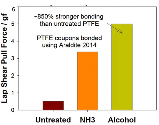
The function of plasma surface modification of polytetrafluoroethylene (PTFE) is to provide reactive chemical functions, promote the combination of adhesives and inks, and promote the molecular binding of biocompatibility. The adhesion properties of polytetrafluoroethylene (PTFE) were improved more than 8 times by plasma induced ethanol copolymerization. Compared with the ammonia plasma treatment, the process is significantly improved.
The bonding strength of PTFE is directly related to the surface energy and has nothing to do with the actuator (defluorination and surface polarization) which cause the change of surface energy. This is of interest for in vivo applications where low surface energy is required, and specific chemical functions are grafted onto polytetrafluoroethylene. Our
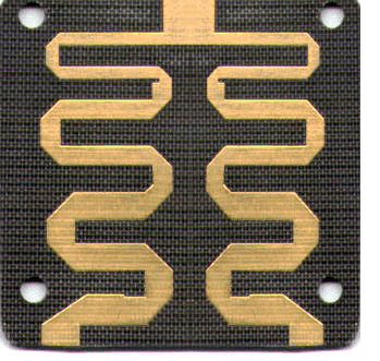
PCB factory must do plasma process when we produce
PTFE PCB after drilling. Otherwise, if we take PCB to PTH process directly, we will not be able to be plating copper and finish hole metallization. Moreover, the PTH process should be completed within 2 hours after the plasma process is completed, otherwise the plasma process will be invalid, which is the manufacturing difficulty of PTFE PCB.