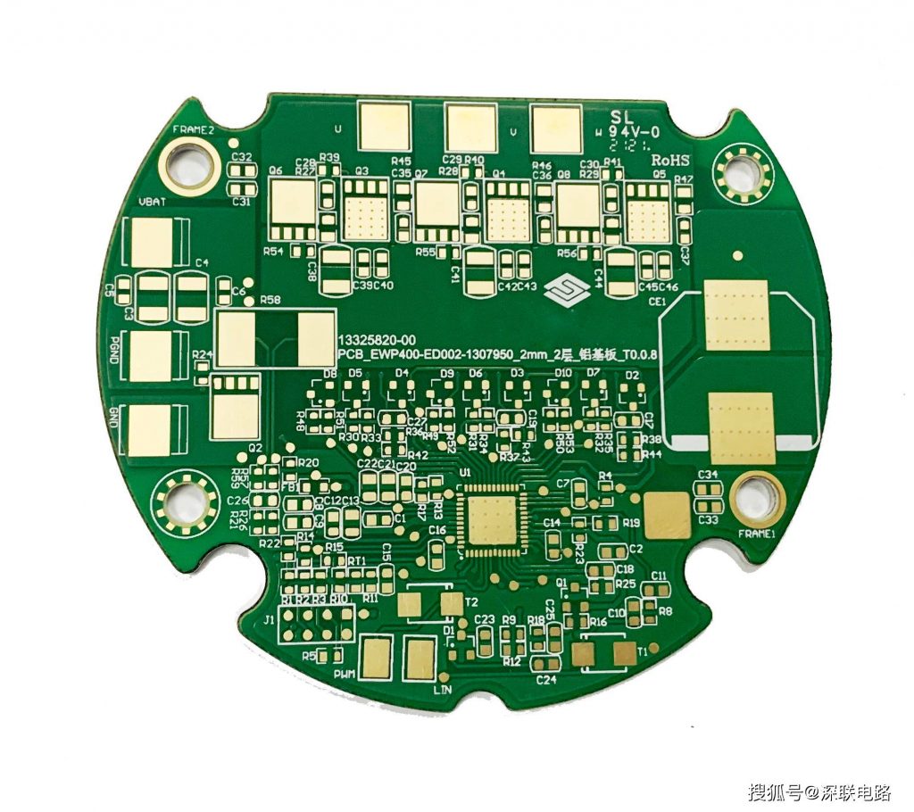
ENIG PCB and flash gold PCB are commonly used in PCB design and PCB production. With the increasing integration of IC, IC pins are more and more dense. However, it is difficult for HASL process to blow even the fine pad, which brings difficulty to SMT assembly; in addition, HASL PCB has a short service life. Flash gold PCB solves these problems. Because the pad flatness is directly related to the quality of solder paste printing process, and has a decisive impact on the subsequent reflow welding quality, the whole board flash gold is often seen in high-density and ultra-small surface mounting process. In the trial production stage, affected by factors such as component procurement, it is not often that the boards are soldered immediately when they come, but that it often takes weeks or even months to use them. The standby life of flash gold PCB is many times longer than that of HASL PCB. In addition, the cost of flash gold PCB design in the sample stage is almost the same as that of lead HASL board.

ENIG is a kind of electroless nickel gold deposition method, which can achieve a thicker gold.
The principle of flash gold is that nickel and gold (commonly known as gold salt) are dissolved in the chemical solution, the circuit board is immersed in the electroplating cylinder and connected with the current to generate nickel gold coating on the copper foil surface of PCB. Because of its high hardness, wear resistance and non oxidation characteristics, electroplated gold is widely used in electronic products.
Differences between ENIG PCB and flash gold PCB in PCB design
1. The crystal structure of ENIG is different from that of flash gold. ENIG is much thicker than gold plating for gold. ENIG will be golden yellow and more yellow than flash gold, which makes customers more satisfied.
2. The crystal structure formed by ENIG and flash gold is different. ENIG is easier to weld than false gold, which will not cause poor welding and cause customer complaints. The stress of ENIG PCB is easier to control, which is more conducive to bonding processing for products with bonding. Also because ENIG is softer than flash gold, ENIG PCB is not wearable.
3. ENIG PCB only has nickel and gold on the pad, and the signal transmission in skin effect is in copper layer, which will not affect the signal.
4. ENIG has more compact crystal structure than flash gold and is not easy to produce oxidation.
5. As the wiring becomes more and more dense, the line width and spacing have reached 3-4mil. Flash gold is prone to short circuit. ENIG PCB only has nickel gold on the pad, so it will not produce gold wire short circuit.
6. ENIG PCB only has nickel gold on the pad, so the bonding between the solder mask and the copper layer is stronger. The project will not affect the spacing when making compensation.
7. It is generally used for boards with relatively high requirements, and its flatness is good. ENIG is generally used, and ing will not appear black cushion after assembly. ENIG PCB has the same flatness and service life as flash gold PCB.

