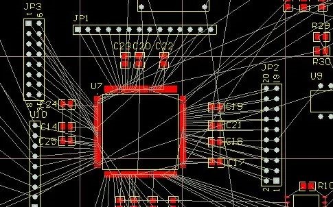
To complete the routing task successfully, the routing tool needs to work under the correct rules and constraints.
To classify all signal lines with special requirements, each signal class should have priority, and the higher the priority, the more strict the rules.
The rules involve: wire width, maximum number of vias, parallelism, mutual influence between signal lines and layer limitation. These rules have a great impact on the performance of wiring tools. Careful consideration of design requirements is an important step for successful wiring.
Layout of components
Design for manufacturability (DFM) rules restrict the layout of components in the process of optimal assembly. If the assembly department allows the components to move, the circuit can be properly optimized to facilitate automatic routing.
For example, for the layout of power lines:
a. In the PCB layout, the power decoupling circuit should be designed near the relevant circuits, rather than placed in the power supply part. Otherwise, the bypass effect will be affected, and the pulsating current will flow through the power line and ground wire, causing interference;
b. For the internal power direction of the circuit, the power supply from the last stage to the front stage should be adopted, and the power filter capacitor of this part should be arranged near the last stage;
c. For some main current channels, such as breaking or measuring current during debugging and testing, the current gap should be arranged on the printed wire during layout.
In addition, it should be noted that the regulated power supply should be arranged on a separate printed circuit board as far as possible. When the power supply and the circuit share the printed circuit board, in the layout, it should be avoided to mix the regulated power supply and circuit components or make the power supply and circuit share the ground wire.
Because this kind of wiring is not only easy to cause interference, but also can not disconnect the load during maintenance, so only part of the printed wire can be cut, thus damaging the circuit board.
Fan out design

In the fanout design stage, each pin of SMD should have at least one via so that the circuit board can carry out inner layer connection, on-line test and circuit reprocessing when more connections are needed.
Manual wiring and key signal processing
Manual wiring is an important process in PCB design now and in the future. Manual wiring is helpful for automatic routing tools to complete the wiring work.
By manually routing and fixing the selected net, we can form the path that can be used for automatic routing. First, route the key signals, either manually or in combination with automatic routing tools.
After the wiring is completed, the relevant engineering and technical personnel will check the wiring of these signals. After passing the inspection, these wires will be fixed, and then the remaining signals will be automatically wired. Due to the existence of impedance in the ground wire, the common impedance interference will be brought to the circuit.
Automatic routing
For the wiring of key signals, it is necessary to control some electrical parameters, such as reducing the distributed inductance, etc. the quality of automatic wiring can be guaranteed to a certain extent after understanding the input parameters of the automatic wiring tool and the influence of the input parameters on the wiring.
The general rules should be adopted in the automatic wiring of signals. The layers and vias used by the given signals can be limited by setting the limiting conditions and the no wiring area. The wiring tools can automatically route according to the design ideas of engineers.
After setting the constraints and applying the created rules, the automatic routing will achieve the expected results. After a part of the design is completed, it will be fixed to prevent the influence of the subsequent routing process.
The number of routing depends on the complexity of the circuit and the number of general rules defined. The current automatic routing tools are very powerful, and can usually complete 100% wiring.
However, when the automatic routing tool has not completed all the signal wiring, it is necessary to manually route the remaining signals.
Arrangement of wiring
For signals with few constraints, the wiring length is very long. At this time, we can judge which wiring is reasonable and which wiring is unreasonable, and then we can shorten the signal wiring length and reduce the number of vias by manual editing.Mastering the above PCB design skills, the PCB designed can facilitate the process of
PCB manufacturing, and the production of PCB Factory is also very simple, so you can’t imagine the happiness of design engineers.

